Conventional Techniques for Microlens Array Fabrication
Conventional Techniques for Microlens Array Fabrication
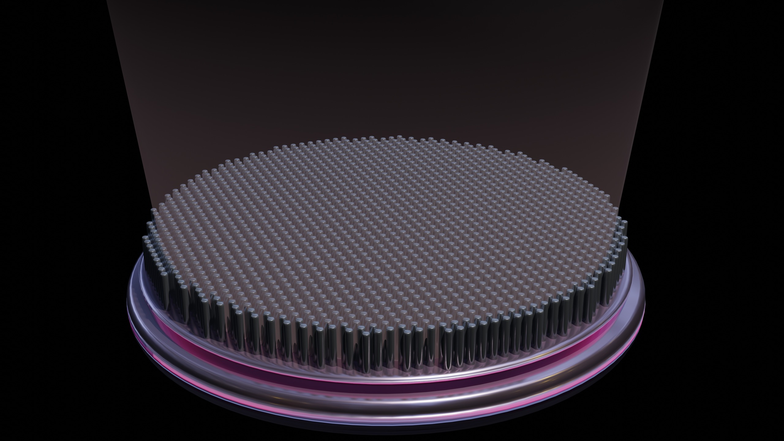
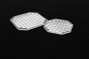
Microlenses are versatile components that modulate light for applications like beam shaping, focusing, and imaging. Advances in mechanical processing, automation, and optics have driven the rapid development of microlens arrays (MLAs), which are used in communications, imaging, sensing, and displays. An MLA is composed of micron-scale microlenses arranged in specific patterns. By adjusting the microlenses’ shape, focal length, and arrangement, designers can achieve desired optical effects. MLAs can be categorized into diffractive, refractive, hybrid (Fresnel), and superlens types based on their light modulation principles.
Standard Techniques for MLA Production
This section outlines conventional MLA production methods, focusing on the established techniques for fabricating MLAs with small areas and millimeter or sub-millimeter apertures.
Ultra-Precision Optical Machining
- Roller Diamond Turning: This method is effective for creating large-scale, continuous microstructures (such as microlens gratings and cylindrical lens gratings) on roller surfaces, with widths reaching meter levels. Due to constraints related to diamond tool size, mechanical precision, and tool wear, producing fine micro-structures smaller than 50 microns remains difficult.
- Single-Point Diamond Turning (SPDT): This technique is used to directly machine large-aperture, small-area microlens molds on metal surfaces. SPDT is suitable for producing microlens arrays with orthogonal and honeycomb patterns and varying focal lengths. While this mature technology works well for conventional apertures ranging from 250 microns to several millimeters, the wear and tear on the tools limit its suitability for large-area applications (inches) and make it challenging to create molds for small-aperture (micron-level) and large-area (tens of inches) MLAs.

Photoresist Melting Method
- Using a photomask, this technique exposes thick photoresist to form circular patterns. After developing, the bottom lines are exposed, and high-temperature baking forms spherical MLAs by utilizing the photoresist’s thermoplastic properties and surface tension. This simple process is effective for fabricating small-area MLAs with apertures ranging from 15 to 100 microns.
- For large-area MLAs (tens of inches), maintaining parallelism between the photomask and the photoresist glass substrate is crucial for consistent exposure, affecting the uniformity of microlens shapes. The melting method’s exposure pattern limits the ability to modify microlens shapes and apertures, making it challenging to achieve a 100% fill factor. Additionally, creating large-area photomasks can be expensive.

3D Printing Techniques
- Inkjet Printing: This method uses UV ink viscosity and the amount of ink dispensed to form microlenses, taking advantage of the surface tension of the ink material. Inkjet printing offers high flexibility and the theoretical capability for large-area production. However, controlling microlens aperture, sag height, and fill factor is difficult, and achieving consistent shapes and focal lengths based on design specifications is challenging. Variability in surface tension and ink volume can significantly impact uniformity, limiting this method to producing simple MLAs that may not meet industrial quality standards.
- Photocuring Micro-Nano 3D Printing: This layered 3D printing approach can produce MLAs with different parameters. However, the low efficiency of micro-nano 3D printing limits its application to small-area microlens mold production, making it more suitable for research settings.
Other Fabrication Techniques
Alternative methods include ultra-self-assembly, which faces challenges in ensuring uniform surface quality across large-area MLAs. Femtosecond laser processing can be categorized into two approaches: two-photon polymerization, which is an additive process for fabricating micro-nano structures using various materials (polymers, metal solutions, biocompatible materials, and graphene oxide), and femtosecond laser ablation, a subtractive process for removing complex structures from hard materials (semiconductors, dielectrics, metals). Currently, these techniques are mainly used for producing small samples and are not yet suitable for industrial-scale production.
Materials Commonly Used in MLA Fabrication
Choosing the appropriate material is a crucial first step in designing and fabricating MLAs. Common materials include polycarbonate (PC), silicon dioxide (SiO2, quartz), photoresist, polydimethylsiloxane (PDMS), polymethyl methacrylate (PMMA), and polyurethane (TPU).
- Optical Plastics: Materials such as polycarbonate (PC), polyurethane (TPU), polyester (PET), and polymethyl methacrylate (PMMA) are frequently used in industrial MLA applications. These materials can be processed using precision injection molding (suitable for high volumes with high mold costs), hot embossing (suitable for low volumes with low mold costs), and UV nanoimprinting (suitable for various volumes with high fidelity).
- Polycarbonate (PC): Ideal for high-temperature environments like automotive applications, PC offers high light transmittance (up to 92%), excellent transparency, and good heat resistance (-40°C to 110°C). It is durable, though its transmittance for short-wavelength light is slightly lower than PMMA.
- Thermoplastic Polyurethane (TPU): TPU is used for applications requiring flexibility, abrasion resistance, and high-temperature stability, such as light-field imaging.
- Polyester (PET): For large-area, cost-effective optical security and display applications, PET optical films can cover areas up to a meter wide. Small MLAs can be made through precision injection molding, while large-area MLAs utilize nickel molds and UV nanoimprinting for high fidelity and low cost.
- Polymethyl Methacrylate (PMMA): PMMA is a transparent thermoplastic polymer with high light transmittance (up to 92%) and excellent transparency. PMMA’s heat resistance and durability are lower than those of PC, but it is inexpensive, has high mechanical strength, and is easy to process. When heated above its glass transition temperature, PMMA exhibits good plasticity, making it suitable for hot embossing. Adjusting the imprinting temperature allows for complete cavity filling.
- Quartz Glass: Quartz glass is used for applications where precise control over MLA size deformation is required, such as imaging. Quartz glass MLAs are typically produced using ion etching or UV optical adhesive replication and are suitable for small-size applications.
- Photoresist Melting: Photoresist materials, which solidify under UV exposure, are characterized by high photosensitivity, curing degree, and speed. These properties make photoresists widely used in inkjet printing and thermal reflow processes for microlens fabrication. SU-8 negative photoresist, with its high transmittance, refractive index, and low polymer shrinkage, is a popular choice for microlens manufacturing. SU-8’s excellent mechanical properties, thermal stability, and optical performance make it suitable for creating micro-optical components. Photoresist MLAs are mainly used for small-scale research.
- Polydimethylsiloxane (PDMS): PDMS is a silicon-based thermosetting polymer with low surface energy and hydrophobic properties. It exhibits good mechanical and thermal performance at high temperatures and provides a smooth surface finish. PDMS prevents polymers from sticking to the mold during demolding, facilitating easy release. It has good transmittance in the visible light range (400-700 nm), with a transmittance exceeding 93%. Due to its elasticity, softness, stability, and optical properties, PDMS is ideal for imprint molds for various polymer microlenses, making it suitable for research applications.
The conventional microlens array fabrication methods discussed above are widely used in scientific research and product development. UV 3D lithography technology offers a promising solution for large-area, small-aperture, and varied numerical aperture (NA) MLAs, providing a new approach to large-scale digital manufacturing.
Contact Shanghai Optics today! We’d be more than happy to discuss your projects and how to best bring them to fruition.

